• Skip navigation
  • Skip to navigation
  • Skip to the bottom
Simulate organization breadcrumb open Simulate organization breadcrumb close
GRK 1896
  • UnivIS
  • Mein Campus
  • StudOn
  • IdM Portal
  • FAU Location Map

GRK 1896

Navigation Navigation close
  • Research
    • Project areas
      • Project area A „Functional Nanostructures and Networks“
        • A1: Structure-property relations of nanowire networks
        • A2: Degradation and corrosion at nanostructures and metal surfaces
        • A3: Growth, stabilization and ripening of nanoparticles in suspensions
        • A4: Growth and characterization of thin single crystalline layers for molecular electronics
        • A5: Degradation and corrosion of metalic nanostructures and nanostructured metals
        • A6: Hybride semiconductors – metal nanowire composites for opto-electronic devices
      • Project area B „Mechanical Properties of Interfaces“
        • B1: Mechanical switching of molecules on surfaces
        • B2: Structural changes in nanoparticles under pressure loading
        • B3: Mechanical properties and fracture behavior of thin layers
        • B4: 3D-deformation behavior of nanoporous metals and nanocomposites
        • B5: 3D-structure-property relations at grain boundaries
        • B6: Influence of topology, interfaces and local chemical compositions on the deformations behavior of nanostructures
      • Postdoc project Z: NanoCT – Developing and establishing of novel in situ approaches
    • Publications
    Portal Research
  • Activities
    • Weekly seminar and events
      • Current schedule
      • Archive
        • 2016
        • 2015
        • 2014
        • 2013
    • International symposium
      • Program
      • Registration
    Portal Activities
  • About us
    • PhD students
    • Supervisors
    • Post-Docs
    • Alumni
    • Contact
    Portal About us
  1. Home
  2. Research

Research

In page navigation: Research
  • Project areas
    • Project area A „Functional Nanostructures and Networks“
      • A1: Structure-property relations of nanowire networks
      • A2: Degradation and corrosion at nanostructures and metal surfaces
      • A3: Growth, stabilization and ripening of nanoparticles in suspensions
      • A4: Growth and characterization of thin single crystalline layers for molecular electronics
      • A5: Degradation and corrosion of metalic nanostructures and nanostructured metals
      • A6: Hybride semiconductors – metal nanowire composites for opto-electronic devices
    • Project area B „Mechanical Properties of Interfaces“
      • B1: Mechanical switching of molecules on surfaces
      • B2: Structural changes in nanoparticles under pressure loading
      • B3: Mechanical properties and fracture behavior of thin layers
      • B4: 3D-deformation behavior of nanoporous metals and nanocomposites
      • B5: 3D-structure-property relations at grain boundaries
      • B6: Influence of topology, interfaces and local chemical compositions on the deformations behavior of nanostructures
    • Postdoc project Z: NanoCT – Developing and establishing of novel in situ approaches
  • Publications

Research

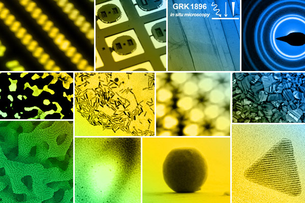
Research into innovative nanostructured materials is of fundamental importance for Germany’s technological competitiveness and in addressing global challenges, like the development of renewable energy sources. Nanostructured materials are controlled by size and interfaces, which give rise to enhanced mechanical properties and new physical effects leading in turn to new functionalities. The design of novel nanostructured materials and devices such as flexible electronics demands state-of-the-art nanocharacterization tools. In particular, methods based on short-wave radiation (electrons, X-rays/neutrons) or scanning probes are ideally suited to analyze materials at the nanometer and atomic scale. Recently developed in situ capabilities and the use of complementary characterization methods allow unique insights into the structure formation, functionality and deformation behavior of complex nanostructures. These new in situ techniques will be the future key tools for the development of new materials and devices.


  • Imprint
  • Privacy
  • Accessibility
Up