Uwe Mick
Dipl.-Phys. Uwe Mick
Max Planck Institute for the Science of Light
Max Planck Institute for the Science of Light (Christiansen Group)
Staudtstr. 2
91058 Erlangen
Germany
- Phone number: +49 9131 7133414
- Fax number: +49 9131 7133990
- Email: uwe.mick@mpl.mpg.de
- Website: https://www.mpl.mpg.de/en/institute/the-institute/
Project description
The atomic force microscope (AFM) has become a proven tool to manipulate nano-objects such as particles or wires. However, as a stand-alone technology it lacks direct feedback about the progress and success of any intended manipulation action. And using the AFM for manipulations with intermitting AFM scanning itself to evaluate such manipulation steps, quickly becomes a time-consuming, slow and inefficient approach, especially for more complex and ambitious manipulation purposes. Furthermore, if one intends to perform more complex nanomanipulation objectives such as controlled pick-and-place handling of nano-objects, the AFM especially cannot provide easy feedback if an intended manipulation was successful. And it especially cannot tell a user, what happened, if the manipulation failed. The scanning electron microscope (SEM), in contrast, permits an almost real-time observation of nanoscale sceneries with reasonable video-rates up to a few frames per second and could provide the much needed visual feedback for nanoscale manipulations.
Therefore, this project aimed for developing a dedicated manipulation setup that would combine the unsurpassed nanomanipulation capabilities of an AFM with the immediate visual feedback of an SEM on said manipulation techniques to facilitate quick, efficient and well controlled nanomanipulation processes. Furthermore, since the visual feedback would also permit direct in-progress feedback about nanomanipulations, it also enables more complex and ambitious manipulation procedures such as selecting and collecting nanoparticles from a reservoir and transferring them in a pick-and-place fashion onto dedicated target samples or even target devices.
One of the background motivations for this project was that a large variety of wet-chemically synthesized nanoparticles and nano-objects are in principle available, even including more complex nanoparticles such as core-shell structures. A dedicated manipulation technique that would permit to selectively assemble even complex particles patterns from such nanoparticles in a precise and individually controlled fashion would provide experimental access to nanopatterns that could not be built otherwise and especially neither with conventional lithography approaches nor with today’s self-assembling techniques. As a serial manufacturing technique such a manipulation system as developed here can only provide a rapid-prototyping approach of individual patterns but not a high-throughput mass fabrication. Nevertheless, if the objective for example is to investigate only individual nanopatterns and their individual interactions with highly focused light fields, as it is the case in the Max-Planck-Institute for the Science of Light, then such a manipulation technique becomes a valid and valuable approach for fabricating and rapidly prototyping individually and geometrically well-controlled nanoparticle assemblies, and especially heterogeneous ones, for plasmonics research, optoelectronics and even device prototyping.
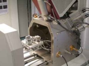
Fig. 1: The dedicated nanomanipulation setup is mounted on the stage of an SEM. In the upper right corner the electronic connectors can be seen to control its 13 degrees of freedom for actuation.
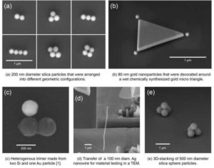
Fig. 2: A medley of various nanoparticle patterns that were fabricated with the setup to illustrate its nanomanipulation capabilities.