Nadine Schrenker
Nadine Schrenker, Dr.-Ing.

Department of Materials Science and Engineering
Institute of Micro- and Nanostructure Research and Center for Nanoanalysis and Electron Microscopy (CENEM)
Cauerstr. 6a
91058 Erlangen
Germany
- Phone number: +49 9131 85-64061
- Fax number: +49 9131 85-28602
- Email: nadine.schrenker@fau.de
- Website: http://www.em.techfak.uni-erlangen.de/
Project description
Organic (opto)electronics have undergone a rapid development in recent years. Applications are for instance organic solar cells (OSCs), flexible displays or “smart clothing”. For such applications it is decisive that the active layers as well as the electrodes withstand mechanical loading. Indium tin oxide, which is still a common material as electrode, behaves brittle under deformation and is relatively expensive. Metallic nanowire networks, especially silver nanowires (AgNWs), are highly promising alternatives 1,2. They fulfill the requirement of a low sheet resistance combined with high transmittance. On a macroscopic scale bending tests as well as tensile tests revealed the excellent performance of Ag NW films 3,4.
In order to understand failure mechanisms and prospectively optimize the deformation behavior of AgNW electrodes in situ mechanical testing in the TEM is conducted. In situ tensile tests of single Ag NWs as well as of AgNW networks networks on different flexible substrates such as PEDOT:PSS and PET, which are both used for flexible OSCs, were performed. On a nanometer scale tensile tests of single 5-fold twinned Ag NWs show a ductile behavior and a size effect of the strength. In situ testing reveals nucleation and propagation of partial dislocations during straining. Tensile tests of Ag NW networks in the TEM provide direct insights in the behavior of the network as well as the response of the whole AgNW polymer composite (Fig. 1(a)). A map of the local strain was determined via digital image correlation and depicts a homogeneous strain distribution (Fig. 1 (b)). The fracture behavior of the Ag NWs is ductile (Fig. 1 (c,d)), whereas the PEDOT:PSS film fracture appears to be rather brittle. Since the interaction of mechanical and electrical properties is crucial for applications in (opto)electronics, we are currently working on combining in situ mechanical and electrical measurements in the TEM.
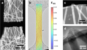
Figure 1. (a) STEM image of an Ag NW network on a PEDOT:PSS film after fracture of an in situ tensile test in the TEM. (b) Determination of the local strain of the sample shown in (a) via digital image correlation). (c) and (d) depict the ductile fracture of the Ag NWs.
References
[1] F. Guo et al., Energy Environ. Sci. 8 (2015) 1631.
[2] S. Yao, & Y. Zhu, Adv. Mater. 27 (2015) 1480.
[3] K.-H. Ok et al., Sci. Rep. 5 (2015) 9464.
[4] F. Nickel et al., Sol. Energy Mater. Sol. Cells 130 (2014) 317.