Ke Ran
Dr. rer. nat. Ke Ran

Former: Department of Materials Science and Engineering
Former: Institute of Micro- and Nanostructure Research and Center for Nanoanalysis and Electron Microscopy (CENEM)
- Email: ran@gfe.rwth-aachen.de
Project description
Former project: Investigation of electrical and mechanical properties of nanomaterials by in situ transmission electron microscopy
Project area: Z
Supervisor: Prof. Dr. rer. nat. habil. Erdmann Spiecker
Metal-organic-semiconducting charge-transfer complexes based on (7,7‘,8,8‘)-Tetracyanoquinodimethane (TCNQ) are regarded as attractive building blocks for molecular electronic devices, due to their intriguing variety of electrical, optical and magnetic properties [1,2]. Among the most prominent representatives in research are Cu-TCNQ and Ag-TCNQ. Particularly, Ag-TCNQ with its voltage-driven bi-stable resistive switching represents a promising candidate for future information media with high storage density [3]. Aiming to implement this effect in genuine devices, the electrical switching of the material has to be understood on small scales. Therefore, we utilized in situ electrical measurements in the transmission electron microscope (TEM) to systematically determine the inherent electronic properties of a larger number of individual Ag-TCNQ nanowires (NWs) (Fig. 1). Electrical switching was successfully induced for tens of NWs upon negative bias sweeps, without the effort of preparing an extra device for each characterized NW. Fitting with Schottky emission function correlated the experimental results with the proposed switching mechanism, and a qualitatively interpretation can be achieved [4].
Wurtzitestructured NWs, such as ZnO, GaN and InN, have attracted extensive research interests, as building blocks for nanogenerators [5], nanosensors [6] and a series of electronic devices [7]. The concept of self-powered and wireless nanotechnology was first proposed by means of ZnO NW arrays in an atomic force microscope (AFM) [5]. Relying on the unique coupling of semiconducting and piezoelectric (PZ) properties of ZnO as well as the Schottky barrier formed at the ZnO-AFM tip interface, nanoscale mechanical energy can be efficiently converted to electrical energy. Following the same principle, high output was achieved in GaN NW arrays based nanogenerators as well, under a forward biased Schottky barrier condition with accumulated PZ potential. Using an in situ AFM-TEM holder (Nanofactory), we had the chance for the first time to explore inside a TEM, the power conversion process from individual GaN NWs (Fig. 2). Single GaN NWs with particular polarity can be selected, and deformed in a controllable way. During the deformation, both electrical and mechanical behaviour of the NW was monitored. Together with finite element method (FEM) simulation, we are aiming to understand the power conversion mechanism and predict the most efficient way to conduct this power conversion.
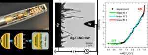
Fig. 1: Experimental setup for the investigation of single Ag-TCNQ nanowires and a successfully induced electrical switch.
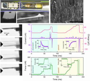
Fig. 2: Experimental setup for the energy conversion study on single GaN nanowires and one example showing the deformation of the nanowire together with the corresponding current and force measurement.
References
[1] H. Alves et al., Nat. Mater. 7 (2008) 574.
[2] J. B. Torrance et al., Solid State Commun. 17 (1975) 1369.
[3] Z. Y. Fan et al., IEEE T. Nanotechnol. 4 (2005) 238.
[4] K. Ran et al., Nanotechnol. 27 (2016) 425703.
[5] Z. L. Wang et al., Science 312 (2006) 242.
[6] J. Zhou et al., Nano Lett. 8 (2008) 3035.
[7] J. H. He et al., Adv. Mater. 19 (2007) 781.