Growth of organic nanocrystals revealed
Crystals are not necessarily hard and resistant but also occur in soft matter when weakly bound molecules arrange in a regular order. Such organic crystals are widespread in pharmaceuticals products, but also occur as tiny nanocrystals in the active layer of organic solar cells. Here, the organic nanocrystals constitute the key ingredient for conversion of light into electricity. In order to enhance the efficiency of such solar cells annealing processes are required to grow the nanocrystals to an optimal size. The problem is that none of the existing microscopy technique enabled direct observation of the growth of such nanocrystals.
Now, a team of scientists at Friedrich-Alexander Universität Erlangen-Nürnberg (FAU) headed by Dr. Mingjian Wu and Prof. Erdmann Spiecker from the Center for Nanoanalysis and Electron Microscopy (CENEM) and supported by a colleague from Lawrence Berkeley National Laboratory (LBNL), USA, developed a novel electron microscopy technique which makes it possible to not only reveal the nanocrystals and their internal molecular order but also directly follow their structural evolution upon annealing. The corresponding publication just appeared in the renowned journal Nature Communications.
“The great challenge that we had to overcome was the extremely high beam-sensitivity of the organic nanocrystals, a quite general feature of molecular crystals. You can only use a few electrons for studying the molecular order before it is destroyed”, explains Prof. Spiecker, head of CENEM and of Institute of Micro- and Nanostructure Research at Department of Materials Science. “On the other hand, only electron microscopy provides sufficient resolution to study individual nanocrystals down to molecular scale.”
A new optical setup: 4D scanning confocal electron diffraction (4D-SCED)
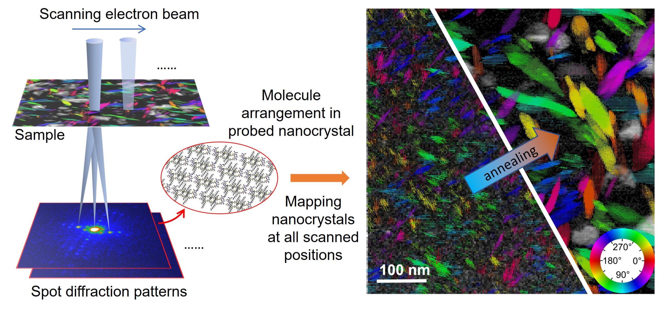
In order to get the most information out of the few electrons available the researchers introduced a new optical setup which they named 4D scanning confocal electron diffraction (4D-SCED). In this technique the electron beam is not directly focused onto the sample, as is usually done, but rather the sample is slightly lifted up so that the cross-over of the beam appears below. “The molecular planes of the nanocrystals act as an optical lattice for the electrons. The electrons are diffracted and generate a spot pattern in the cross-over plane which carries the important information on the molecular order”, says Dr. Wu who elaborated the 4D-SCED technique at CENEM’s cutting edge microscopes. After magnification the spot pattern is captured with a fast camera enabling acquisition of tens of thousands of patterns, which are synchronized with the beam at each point while it raster scans across the sample. From this huge four-dimensional (4D) data set a mapping of the nanocrystals and their molecular order can be extracted. “The key advantage of our technique results from the combination of a slightly defocused beam in the sample plane and the concentration of intensity in the spot pattern captured by the camera”, Dr. Wu explains. “This makes the technique way more dose-efficient than earlier approaches.”
New cutting-edge transmission electron microscope
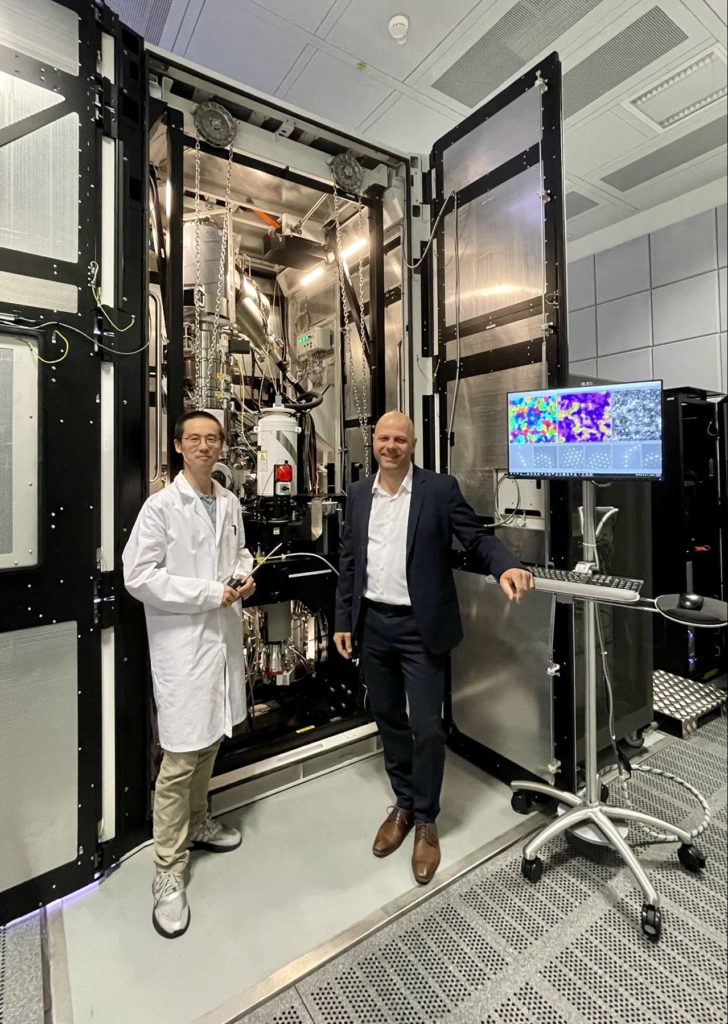 Dr. Mingjian Wu and Prof. Erdmann Spiecker in front of the new probe-corrected Spectra 200 transmission electron microscope
Using CENEM’s excellent microscopes and equipment the researchers applied the 4D-SCED technique together with in situ sample heating to the study of organic nanocrystals in the active layer of an organic solar cell. The 4D-SCED technique is not limited to the study of organic nanocrystals in solar cells but can be applied to all kinds of molecular and polymer crystals, but also to inorganic crystals whenever severe beam damage impedes microscopic investigation of local atomic/molecular order. The development of the 4D-SCED technique was supported by the Collaborative Research Center CRC953 “Synthetic Carbon Allotropes” and the Research Training Group RTG1896 “In situ microscopy with electrons, X-rays, and scanning probes”, two collaborative research projects funded by the German Research Foundation (DFG). Moreover, with the support of the Cluster of Excellence “Engineering of Advanced Materials”, a new cutting-edge transmission electron microscope could be installed and put into operation end of 2020 which already played a vital role in the development of the 4D-SCED technique.
Further information
- , , , , , :
Seeing structural evolution of organic molecular nano-crystallites using 4D scanning confocal electron diffraction (4D-SCED)
In: Nature Communications 13 (2022), Article No.: 2911
ISSN: 2041-1723
DOI: 10.1038/s41467-022-30413-5
BibTeX: Download
Dr. Mingjian Wu, Prof. Dr. Erdmann Spiecker
mingjian.wu@fau.de, erdmann.spiecker@fau.de
Institute of Micro- und Nanostructure Research (IMN) &
Center for Nanoanalysis and Electron Microscopy (CENEM)
Department of Materials Science
Interdisziplinäres Zentrum für Nanostrukturierte Filme (IZNF)
Friedrich-Alexander-Universität Erlangen-Nürnberg
Cauerstraße 3, 91058 Erlangen