In situ microscopy – a key to unravel growth and functional properties of nanowires
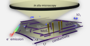
both hold great promise for applications in nanotechnology, ranging from energy storage to microelectronics. In a recent work “Transforming layered MoS2 into functional MoO2” by CENEM researchers Lilian Vogl, Peter Schweizer, Mingjian Wu and Erdmann Spiecker, published in Nanoscale, a novel approach is presented to synthesize molybdenum dioxide nanowires directly from molybdenum disulfide, going from a 2D transition metal chalcogenide to a transition metal oxide nanostructure. This opens a new possibility to direct integrate the unique functional properties of the two classes of materials.
As a topic of the GRK 1896 along the exploration of phase transition and stability of thin film systems (click here to see related studies), the research is featured by the application of in situ microscopic techniques, which allowed not only to observe and understand the growth process and character but also the studies of functional properties, including electric conductance, field emission and mechanical properties, on single nanowire basis. Based on the existing platform of in situ microscopy at IMN/CENEM, Ms. Lilian Vogl with colleagues has further developed and implemented a heating reactor stage compatible to advanced optical microscope with atmospheric flux controllers in course of the study. The capability to directly observe the reaction process was the key to reach a good control of shape, morphology and crystal phase of the reaction products. Systematic analysis of the observation footage even revealed the growth kinetics. While ex situ observations in the transmission electron microscope (TEM) elaborated the crystal structure, chemical composition and distribution down to atomic scale, which shed light to understand the details of growth process.
Further highlights of the research are the development of in situ techniques in the scanning electron microscope (SEM) with advanced manipulators and controller systems. This has enabled measurements of conductance of MoO2 single nanowire and junction of nanowires to be measured with four-probe methods, and the nano-mechanical properties being scooped by the electro-resonance measurements. Last-but-not-least, the field emission properties of single MoO2 nanowire was tested in the TEM.
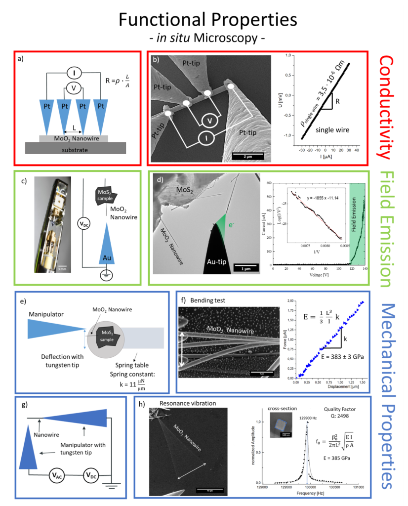
The functional properties, including conductivity, field emission and mechanical properties, are studied on single wire basis by applying in situ observation/manipulation techniques in the SEM/TEM.
The paper is published recently in the Nanoscale, and can be visited via the link here (and metadata below). Congratulations, Lili and colleagues!
- , , , :
Transforming layered MoS2 into functional MoO2 nanowires
In: Nanoscale 11 (2019), p. 11687-11695
ISSN: 2040-3364
DOI: 10.1039/c9nr03346g
BibTeX: Download